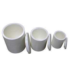
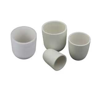
A new generation of boron nitride ceramic crucibles is now available for melting high purity gallium used in compound semiconductor production. These crucibles offer exceptional performance where traditional materials fall short. Gallium is a key element in making advanced semiconductors for electronics and optoelectronics. It must stay pure during the melting process to ensure the final product works as intended. Boron nitride ceramics meet this need because they do not react with molten gallium. They also resist thermal shock and maintain stability at high temperatures.
(Boron Nitride Ceramic Crucibles for Melting High Purity Gallium for Compound Semiconductor Production)
Manufacturers face challenges when handling gallium because it can stick to or corrode many container materials. This leads to contamination and wasted material. Boron nitride solves these problems. Its non-wetting surface keeps gallium from sticking. Its chemical inertness prevents unwanted reactions. Both features help maintain the metal’s purity from start to finish.
The new crucibles are made using advanced hot-pressing techniques. This gives them a dense, uniform structure without open pores. As a result, they last longer and perform more reliably than older versions. Semiconductor producers can now run their processes with fewer interruptions and less risk of defects.
(Boron Nitride Ceramic Crucibles for Melting High Purity Gallium for Compound Semiconductor Production)
These improvements come at a time when demand for high-performance semiconductors is rising fast. Devices like 5G components, power electronics, and LED systems all rely on clean, consistent gallium-based materials. Using boron nitride crucibles supports better yields and higher quality in these critical applications. Companies adopting this technology report smoother operations and reduced downtime during production runs. The crucibles are compatible with standard melting setups and require no major changes to existing workflows.