1. Crystal Framework and Polytypism of Silicon Carbide
1.1 Cubic and Hexagonal Polytypes: From 3C to 6H and Beyond
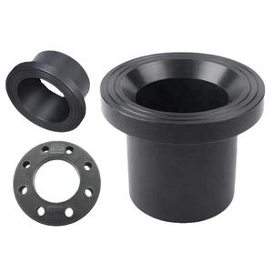
(Silicon Carbide Ceramics)
Silicon carbide (SiC) is a covalently bound ceramic made up of silicon and carbon atoms arranged in a tetrahedral coordination, forming one of one of the most complicated systems of polytypism in products scientific research.
Unlike most porcelains with a single stable crystal framework, SiC exists in over 250 known polytypes– unique piling series of close-packed Si-C bilayers along the c-axis– ranging from cubic 3C-SiC (additionally known as β-SiC) to hexagonal 6H-SiC and rhombohedral 15R-SiC.
The most typical polytypes utilized in engineering applications are 3C (cubic), 4H, and 6H (both hexagonal), each showing somewhat different digital band frameworks and thermal conductivities.
3C-SiC, with its zinc blende framework, has the narrowest bandgap (~ 2.3 eV) and is typically expanded on silicon substrates for semiconductor devices, while 4H-SiC provides exceptional electron flexibility and is preferred for high-power electronics.
The strong covalent bonding and directional nature of the Si– C bond give remarkable firmness, thermal security, and resistance to sneak and chemical assault, making SiC suitable for extreme setting applications.
1.2 Defects, Doping, and Electronic Residence
Despite its structural complexity, SiC can be doped to accomplish both n-type and p-type conductivity, enabling its use in semiconductor tools.
Nitrogen and phosphorus function as contributor contaminations, introducing electrons into the conduction band, while light weight aluminum and boron work as acceptors, developing openings in the valence band.
Nonetheless, p-type doping performance is restricted by high activation energies, specifically in 4H-SiC, which poses difficulties for bipolar gadget design.
Native problems such as screw misplacements, micropipes, and piling mistakes can weaken device efficiency by serving as recombination centers or leak paths, requiring high-quality single-crystal growth for digital applications.
The wide bandgap (2.3– 3.3 eV depending upon polytype), high breakdown electrical area (~ 3 MV/cm), and exceptional thermal conductivity (~ 3– 4 W/m · K for 4H-SiC) make SiC much superior to silicon in high-temperature, high-voltage, and high-frequency power electronic devices.
2. Processing and Microstructural Design
( Silicon Carbide Ceramics)
2.1 Sintering and Densification Strategies
Silicon carbide is inherently difficult to densify due to its strong covalent bonding and low self-diffusion coefficients, requiring innovative handling approaches to attain complete thickness without ingredients or with very little sintering help.
Pressureless sintering of submicron SiC powders is possible with the enhancement of boron and carbon, which advertise densification by removing oxide layers and boosting solid-state diffusion.
Hot pressing applies uniaxial pressure throughout heating, enabling full densification at lower temperatures (~ 1800– 2000 ° C )and generating fine-grained, high-strength parts suitable for cutting tools and wear components.
For huge or complicated shapes, response bonding is employed, where permeable carbon preforms are infiltrated with molten silicon at ~ 1600 ° C, forming β-SiC in situ with very little shrinking.
Nevertheless, residual free silicon (~ 5– 10%) stays in the microstructure, restricting high-temperature efficiency and oxidation resistance over 1300 ° C.
2.2 Additive Manufacturing and Near-Net-Shape Fabrication
Recent advancements in additive manufacturing (AM), especially binder jetting and stereolithography making use of SiC powders or preceramic polymers, make it possible for the construction of intricate geometries previously unattainable with conventional approaches.
In polymer-derived ceramic (PDC) paths, fluid SiC precursors are shaped using 3D printing and then pyrolyzed at high temperatures to yield amorphous or nanocrystalline SiC, usually calling for additional densification.
These techniques decrease machining expenses and product waste, making SiC much more accessible for aerospace, nuclear, and warm exchanger applications where intricate styles improve performance.
Post-processing actions such as chemical vapor infiltration (CVI) or liquid silicon seepage (LSI) are occasionally utilized to improve thickness and mechanical integrity.
3. Mechanical, Thermal, and Environmental Performance
3.1 Strength, Hardness, and Use Resistance
Silicon carbide rates amongst the hardest well-known products, with a Mohs solidity of ~ 9.5 and Vickers firmness exceeding 25 Grade point average, making it highly resistant to abrasion, erosion, and scratching.
Its flexural toughness usually varies from 300 to 600 MPa, depending upon processing technique and grain size, and it preserves stamina at temperatures up to 1400 ° C in inert atmospheres.
Fracture toughness, while modest (~ 3– 4 MPa · m ONE/ ²), suffices for lots of structural applications, specifically when incorporated with fiber support in ceramic matrix compounds (CMCs).
SiC-based CMCs are made use of in wind turbine blades, combustor linings, and brake systems, where they offer weight financial savings, fuel effectiveness, and prolonged life span over metallic equivalents.
Its outstanding wear resistance makes SiC suitable for seals, bearings, pump components, and ballistic armor, where longevity under harsh mechanical loading is crucial.
3.2 Thermal Conductivity and Oxidation Stability
One of SiC’s most important buildings is its high thermal conductivity– as much as 490 W/m · K for single-crystal 4H-SiC and ~ 30– 120 W/m · K for polycrystalline types– going beyond that of numerous metals and enabling effective warm dissipation.
This residential property is essential in power electronics, where SiC devices produce less waste warm and can run at higher power thickness than silicon-based devices.
At elevated temperatures in oxidizing atmospheres, SiC creates a protective silica (SiO ₂) layer that reduces further oxidation, providing excellent ecological durability as much as ~ 1600 ° C.
Nevertheless, in water vapor-rich environments, this layer can volatilize as Si(OH)₄, leading to accelerated deterioration– an essential challenge in gas wind turbine applications.
4. Advanced Applications in Power, Electronic Devices, and Aerospace
4.1 Power Electronics and Semiconductor Devices
Silicon carbide has transformed power electronics by allowing gadgets such as Schottky diodes, MOSFETs, and JFETs that run at greater voltages, frequencies, and temperature levels than silicon equivalents.
These gadgets reduce power losses in electric vehicles, renewable energy inverters, and commercial electric motor drives, contributing to global power efficiency renovations.
The ability to operate at joint temperatures over 200 ° C permits streamlined cooling systems and boosted system reliability.
Furthermore, SiC wafers are utilized as substratums for gallium nitride (GaN) epitaxy in high-electron-mobility transistors (HEMTs), combining the advantages of both wide-bandgap semiconductors.
4.2 Nuclear, Aerospace, and Optical Solutions
In nuclear reactors, SiC is a crucial element of accident-tolerant gas cladding, where its reduced neutron absorption cross-section, radiation resistance, and high-temperature strength boost safety and security and performance.
In aerospace, SiC fiber-reinforced composites are made use of in jet engines and hypersonic vehicles for their lightweight and thermal security.
In addition, ultra-smooth SiC mirrors are employed in space telescopes as a result of their high stiffness-to-density ratio, thermal stability, and polishability to sub-nanometer roughness.
In recap, silicon carbide ceramics represent a foundation of modern-day sophisticated products, integrating phenomenal mechanical, thermal, and digital residential or commercial properties.
With specific control of polytype, microstructure, and processing, SiC remains to allow technical developments in power, transport, and severe atmosphere engineering.
5. Distributor
TRUNNANO is a supplier of Spherical Tungsten Powder with over 12 years of experience in nano-building energy conservation and nanotechnology development. It accepts payment via Credit Card, T/T, West Union and Paypal. Trunnano will ship the goods to customers overseas through FedEx, DHL, by air, or by sea. If you want to know more about Spherical Tungsten Powder, please feel free to contact us and send an inquiry(sales5@nanotrun.com).
Tags: silicon carbide ceramic,silicon carbide ceramic products, industry ceramic
All articles and pictures are from the Internet. If there are any copyright issues, please contact us in time to delete.
Inquiry us